Q.7) The CMOS differential pair circuit shown below is to be designed to have a differential gain...
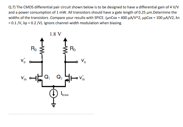
Q.7) The CMOS differential pair circuit shown below is to be designed to have a differential gain of 4 V/V and a power consumption of 1 mW. All transistors should have a gate length of 0.25 um.Determine the widths of the transistors.Compare your results with SPICE. (unCox = 400 A/V^2, Hp Cox = 100 A/V2, An -0.1/V, Ap = 0.2 /V). Ignore channel-width modulation when biasing. 1.8 V RO< RO VO Vin Go, Qrovin
Solved
Electrical Engineering
1 Answer
quang ta
Login to view answer.